


OFERTA FORMATIVA DCM - FCT/UNL
Navigation
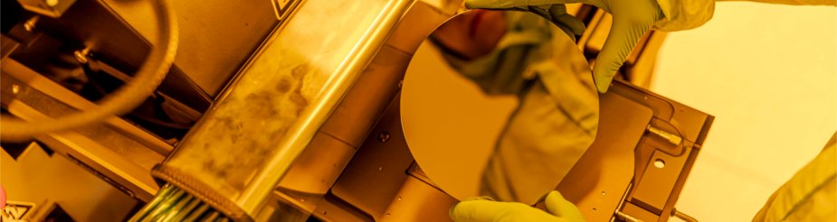
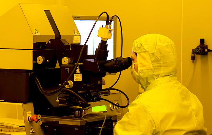
Clean room (Lithography) Lab
Pedro Barquinha (21-2948300 ext. 11605)
Summary description:
The lithography area is an ISO 6 lab devoted to resist patterning and materials etching required to fabricate micro/nanoscale devices. It also includes a LPCVD unit to fabricate polycrystalline Si thin films.
Detailed description:
This lab is equipped with all the required tools to achieve features sizes down to 1 µm (UV Hg lamp), 600 nm (UV laser diode) and 50-100 nm (nanoimprint) in layers composing micro/nanoscale devices. Wafers up to 6” diameter can be processed in spinners (resist deposition and development), hot plates, UV mask aligner, direct laser writer, substrate conformable nanoimprint lithography (SCIL, add-on to the UV mask aligner), wet etching benches and reactive ion etching tools. Available processes can make use of positive and negative tone resists as well as PDMS.
There is also a LPCVD unit to fabricate polycrystalline Si thin films in substrate sizes up to 4”.
|
- Heidelberg µPG 101 Tabletop Micro Pattern Generator - Spinners for resist coating and development - Suss substrate conformable nanoimprint lithography (SCIL) |