


OFERTA FORMATIVA DCM - FCT/UNL
Navigation
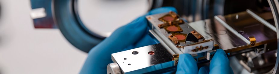
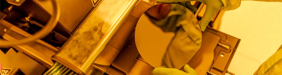
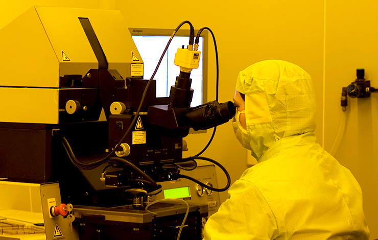
Laboratory of Nanofabrication
- Nanofabrication Laboratory - Scanning Electron Microscopy - Focused Ion Beam (SEM-FIB)
Click here to view the flyer - Nanofabrication Laboratory - Atomic Force Microscopy
Click here to view the flyer - Nanofabrication Laboratory - X-Ray Diffraction XRD Facilities
Click here to view the flyer - Characterization Laboratory - Confocal Laser Scanning Microscope
Click here to view the flyer
SEM-FIB – Zeiss Auriga CrossBeam Workstation
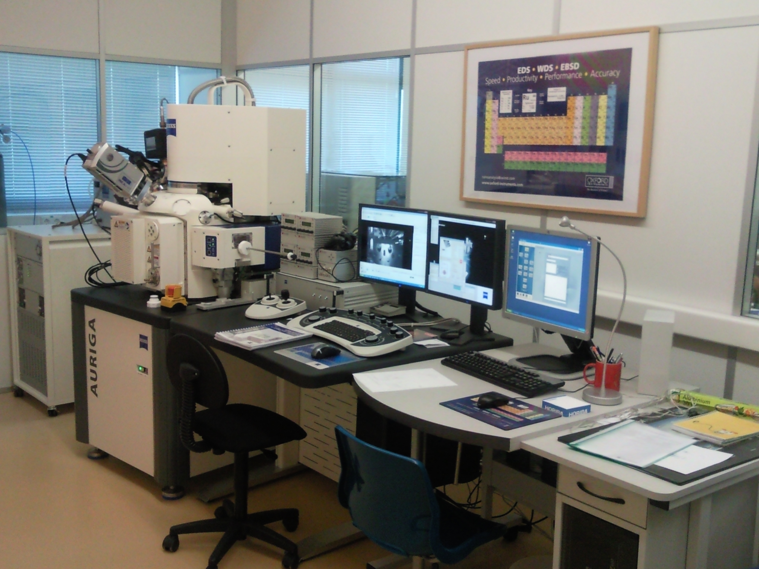
New generation of CrossBeam system allowing for unique imaging possibilities, advanced analytics and precise processing at a nanoscale level.
The main features of the equipment are described below:
- SEM column
- Schottky Field Emitter, resolution of 1.0 nm @ 15 kV, 1.9 nm @ 1 kV, acceleration voltage between 0.1 and 30 kV.
- FIB column
- Ga liquid metal ion source (LMIS), resolution <7 nm @ 30 kV, acceleration voltage between 1 and 30 kV, probe current between 1 pA and 50 nA.
- Imaging with different detectors
- Everhart-Thornley type SE, In-lens SE and BSD detectors. Possibility of 3D reconstruction using combined SEM and FIB columns.
- Microstructural and chemical analysis
- Oxford INCA Energy 350 (EDS), Oxford HKL Advance, Nordlys II-S (EBSD, EBSD 3D).
- Gas injection system
- Deposition of C, Pt and SiO2, selective etching of dielectrics with XeF2, local charge compensation system to reduce charging effects in non-conductive samples.
- Lithography
- Nanolithography using electrons or ions, milling of imported bitmaps or CAD files, electrostatic beam blanker.
- Heating stage
- Kammrat & Weiss, heating up to 1050 °C for in-situ analysis of sample evolution with temperature.
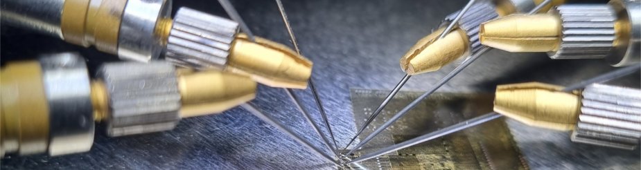
- Nanoprobes
- 4 Kleindiek nanotechnik nanomanipulators for electrical measurements of nanodevices